���� |
by Mitch Jacoby
If a picture is worth a thousand words, then scientists' grasp of molecular electronics has just been expanded by a grand quantity. Researchers at the University of California, Irvine, have recorded the first direct image of a small molecule confined between two metal contacts and have probed its electronic structure systematically, revealing much information about the microscopic junction.
The potential of extremely fast and ultradense electronics based on single molecules as circuit components has motivated many research groups to study the electronic properties of individual molecules. Several teams have created tiny structures that hold a single molecule in a nanometer-sized gap between electrical leads and probed the trapped molecule's electronic conductivity.
But typically, such studies cannot answer unambiguously various questions about the structure and nature of the junction. For example, how does the molecule bond to the metal contacts? Is it attached to both leads? What is its orientation? And what effect does the metal have on the molecule's properties?
UC Irvine physics and chemistry professor Wilson Ho and coworkers have now used a scanning tunneling microscope to position a copper phthalocyanine molecule in the gap between two gold contacts that they constructed one atom at a time. They then recorded high-resolution images of the junction [Science, published online Sept. 4, http://www.sciencemag.org/cgi/content/abstract/1088971v1].
In addition, by altering the length of the gold leads on an atomic scale, the Irvine team was able to study the effect of the metal on the system's electronic density of states.
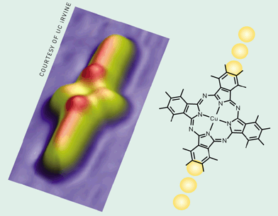 PICTURE THIS With atomic-scale dexterity, UC Irvine scientists have used a scanning tunneling microscope to place a copper phthalocyanine molecule between tiny gold leads and
to image the bridge. PICTURE THIS With atomic-scale dexterity, UC Irvine scientists have used a scanning tunneling microscope to place a copper phthalocyanine molecule between tiny gold leads and
to image the bridge.
| |